Deep Dive into Crystals
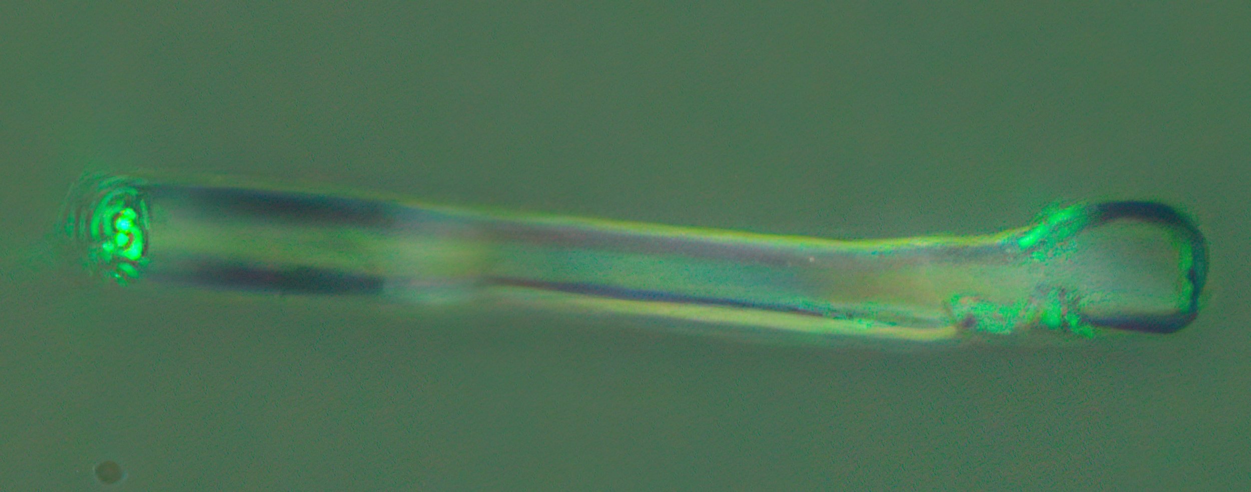
At the nano scale, you might be amazed by what you find, features like valleys and plateaus that resemble the Grand Canyon or desert landscapes. The tiny, nano details are just as remarkable and detailed as what we see on a human scale. By examining crystals, from diamonds to salt, we can uncover long-standing mysteries. Even with the strongest supercomputers, modeling electron flow in a 3 mm diamond wafer is a tough challenge in which you need wet lab data.
By identifying surface defects and linking them to issues in the crystal structure, we can understand how stress affects the electrical properties of semiconductor materials. We're collaborating with scientists and partners to explore the rich world of optical super resolution and the incredible structures of crystals. If you're interested in speeding up the discovery of crystal properties for advanced semiconductors, reach out to us.
AI Detection of Defects
Platelets, hills, holes, defects
NanoFraction technology can identify defects on the surface of diamond wafers in real-time. AI prediction engine can determine electrical properties. Data products on geometry, stress field, and defect density types.
3D Data on Dislocations
Spiral dislocations, threaded dislocations, aggregated
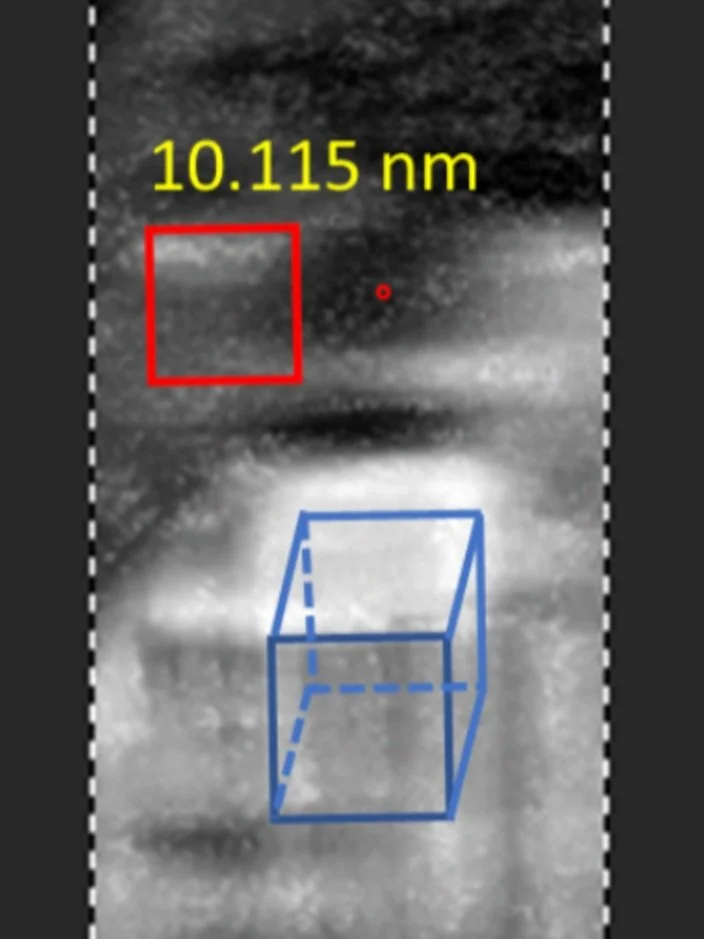
If a more detailed understanding of the defects and dislocations in the crystal is needed NanoFraction technology can visualize 3D nano scale structures. This can uncover a wide range of architectural information that is critical to dynamic behaviors in materials. Crystal defects can often exhibit mobility as a result of stress fields.
Atomic super resolution
NaCl Ions
NanoFraction is benchmarking experimental quantum results with the top tier vision models to push the boundaries of AI super resolution. With our AI super resolution models we have been able to see ions in sodium crystals. If these results are further verified through our R&D we will have set a new standard for optical resolution to the angstrom scale.


