

Non-Destructive Nanoscale Metrology for Advanced Materials
Screen wafers, films, crystals, and manufactured surfaces for defects, topography, roughness, stress, and structural variation—without coating, sectioning, vacuum, or destructive sample preparation.
Label-free optical measurement
Large-area, high-throughput screening
3D surface and defect data
Designed to complement SEM, TEM, AFM, and Raman
Take a closer look at diamond.
Explore a diamond scan from NanoFraction’s image library. Open the interactive viewer to pan, zoom and move through the available detail views.

Select “Explore diamond scan” to load the interactive image.
Digital zoom enlarges the displayed image; it does not establish spatial resolution or validate a defect classification. See the case study for measurement context.
Our Services
Ship us your samples, view results quickly, and share online.

diamond 200 µm
Semiconductors
Diamond, Silicon Carbide, GaN, Graphene
Macro, micro, and nano characterization of advanced materials for semiconductors. Library of AI models for crystal lattice materials.
Data products:
3D geometry
bending radius
maximum stress/strain field
surface roughness
defect and dislocation detection

PETG 200 mm
Advanced Manufacturing
PLA, PETG, ABS, Carbon, Nylon, SLA, PVA, TPU, Metal
Macro, micro, and nano characterization of materials used for Advanced Manufacturing. Multi-scale characterization of infill patterns, thermal properties, stress/strain fields. Prediction engine material library.
Data products:
3D geometry
stress/strain field
defect detection
failure analysis
surface roughness

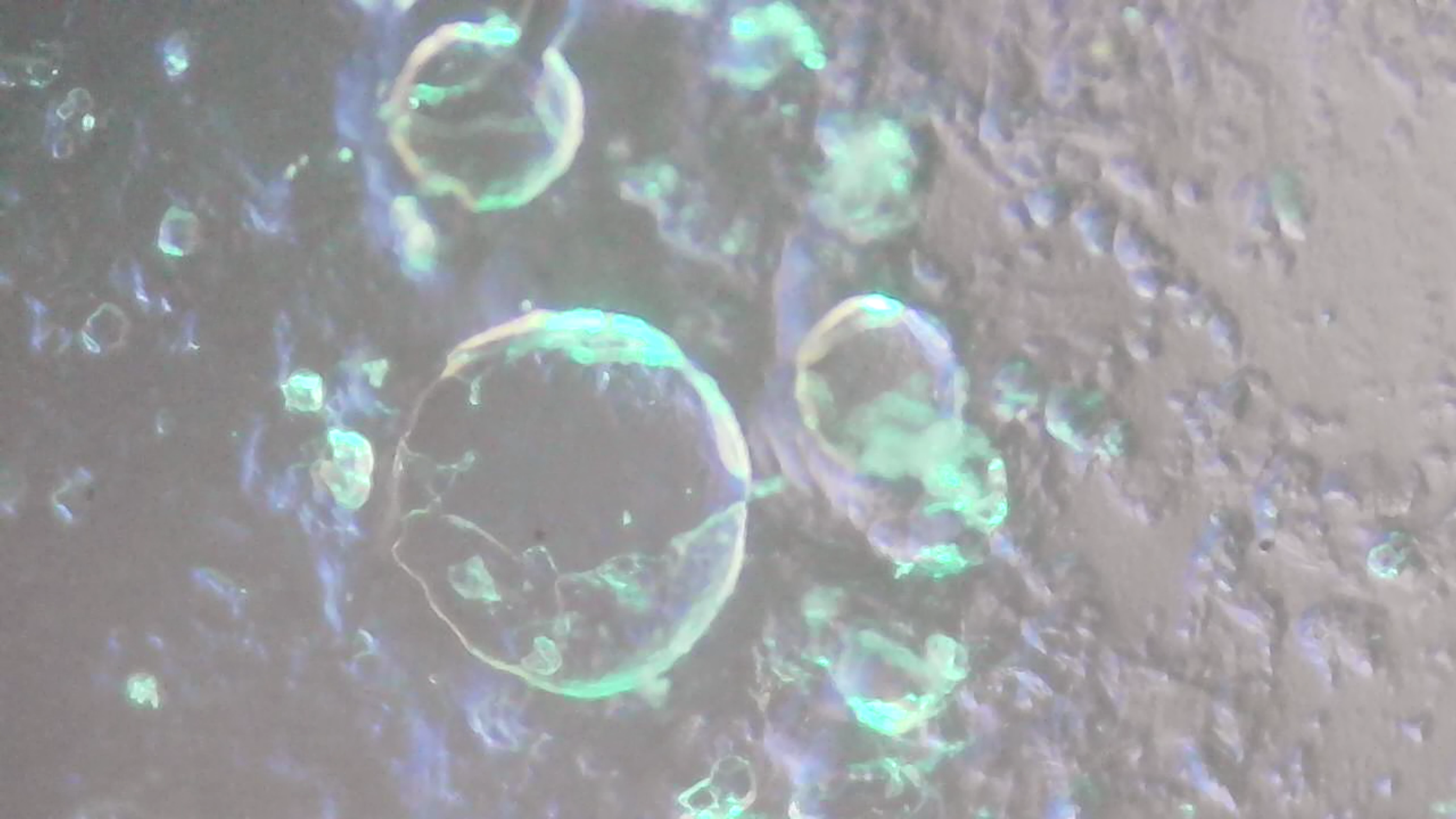
SARS-CoV-2 200 nm
Life Sciences
SARS-CoV-2, TMV, Zebrafish, NaCl
Understanding the architecture of nano-virion including Hepatitis C and SARS-CoV-2 are essential for research and therapeutics. NanoFraction technology is capable of recording nano-scale live cell interactions in situ without the need for labeling, chemical alteration, or cryogenics.
Data products:
3D Geometry
mechanotransduction/ion field
stress/strain field
live cell recording
Years of Science driven by AI & Robotics
From micro meteorites to nano salt crystals, NanoFraction’s service features a modern web-base collaborative platform that facilitates interdisciplinary research, enabling scientists to share insights and resources seamlessly.
Our robotic capture systems implement high-throughput AI screening methods allowing for rapid testing and quality control of nanoscale materials, propelling the pace of discovery and testing.


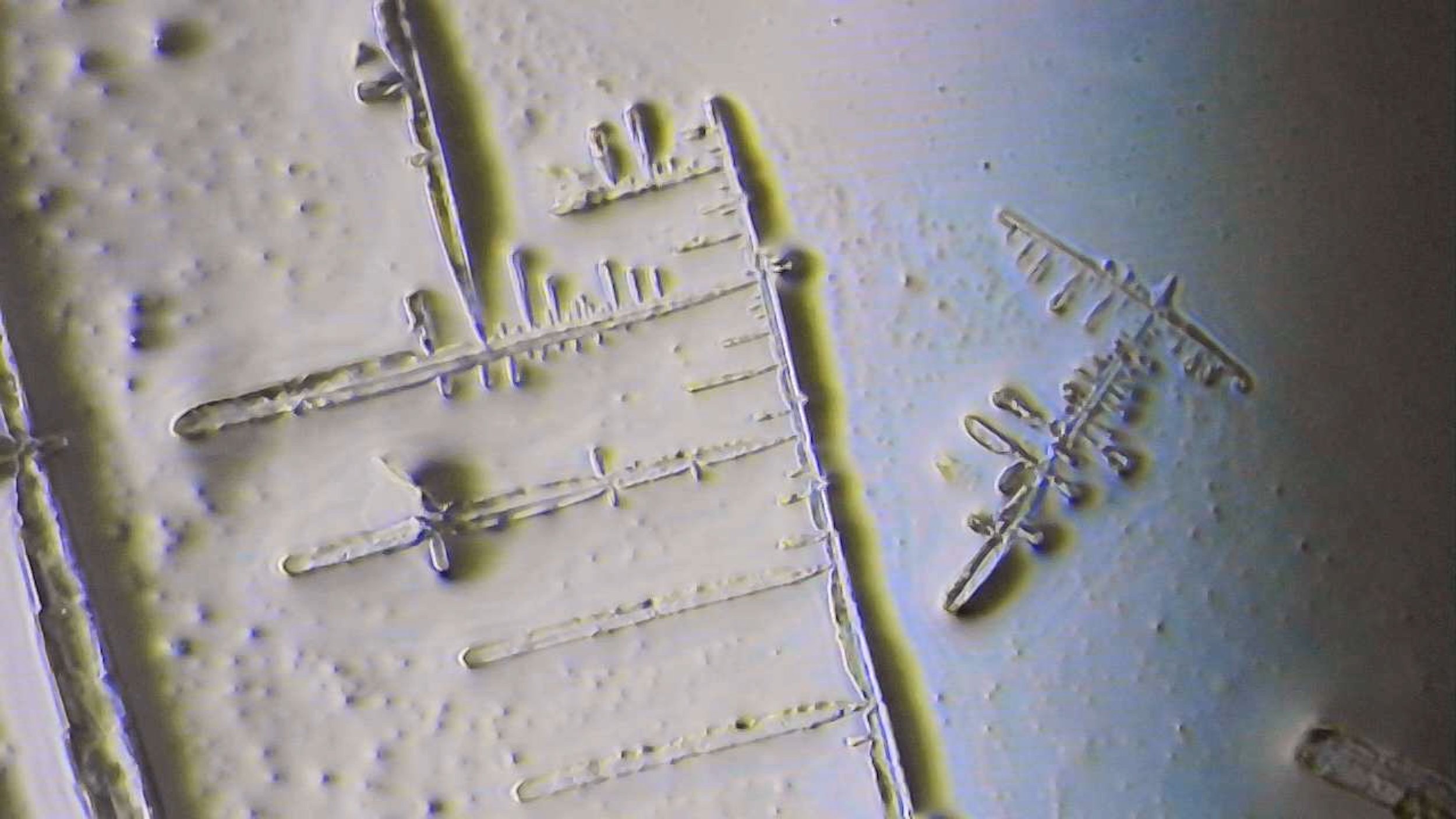
Nano Salt Crystal
-
This data set demonstrates NF capability to capture a 600 nano meter salt crystal from evaporation. In a single image data is captured from hundreds of nanometers to tens of angstroms.
-
By leveraging our AI model for NaCl we are able to apply post capture super resolution machine learning solutions to visualize ions that make up the atomic composition of the salt crystal lattice.

Human Sweat
-
NanoFraction is collaborating with researchers to understand the nano composition of human sweat. Until now it has been impossible to study this important bio marker in a natural condition.
-
It has been discovered that human cells make crystals to store energy and protein. Some biomarkers crystallize outside the body. Understanding the dynamics of cell crystals is an ideal application of NanoFraction technology.

Thermal Metrology
-
The boundaries between light and sound intersect and cross-over when electromagnetic waves pass through materials. NanoFraction technology can measure the ultrasound waves arising from this interaction. This data can be used for thermal analysis of materials.
-
Underlying NanoFraction technology is an AI physics engine that is based on analytic operators that connect the quantum world to the classical world of mechanics. This allows NanoFraction to simulate and compare with actual experimental results.





-
![Seal of Politecnico di Bari featuring a lion in the center, surrounded by Latin text and geometric design.]()
Science Collaborator
-
![Logo of Southern University featuring a roaring lion with a mane, in black and gold colors, with the words 'Southern University' in bold green and white text.]()
Science Collaborator
-
![Logo for General Stress Optics featuring the initials GSO in bold black letters with the full company name below.]()
Solutions Partner
-
![Hirox logo in white text on a black background.]()
Solutions Partner
-
![Dover Motion logo with three rightward arrows and the text 'A division of Invetech'.]()
Solutions Partner
-
![A stylized tree with a spiral at the center, surrounded by multiple leaves and small decorative stars. Below the tree, the text reads "TEKNA SOLUTIONS" in bold.]()
Solutions Partner


Contact Us
Interested in working together? Fill out some info and we will be in touch in a nano second. We can’t wait to hear from you!
We work on a services first, hardware second model.
Provided your target is well suited for our technology, we will first build a research program and data analysis workflow around your area of interest.
At our second stage we can provide access to our hardware systems based on the requirements of your application.